Light Conversion using Perovskite Quantum Dots
Introduction
Sometimes it is not the chemical composition that defines the properties of a material, but its shape and size. This is the case for small semiconducting particles, commonly called quantum dots. The dimension and shape of these nanocrystals make them uniquely versatile and promising for electro-optical applications.
Quantum dots are crystalline semiconductor particles, with a radius of few nanometers, whose optical and electrical properties are essentially determined by the size. The smaller the particles, the more the optical absorption and emission shift towards shorter wavelengths.
This blog post describes some of the properties and applications of quantum dots, in particular perovskite nanocrystals. We are showing how to characterize films with embedded nanocrystals using angular resolved electroluminescence (Phelos) and analyze the results with a fully coupled electro-optical simulation (Setfos).

Fig. 1. Emission from UV-illuminated quantum dots. The color of the solution depends on the quantum dot size. Small quantum dots emit violet light, whereas larger ones emit red light. Source: Wikipedia, (CC BY-SA).
Due to their small size, charge carriers in quantum dots are confined to a small area. The confinement is on the same scale as the particles themselves, which is on the order of a few nanometers. Therefore, the behavior of charge carriers is dominated by the laws of quantum mechanics. This means that charge carriers are only allowed on discrete energy levels. This is similar to atoms, where electrons have a clearly defined set of discrete energies. These discrete energy levels are seen in the absorption and emission spectra and are the reason quantum dots are also called artificial atoms. The energy levels and their separation can be tuned by varying the size of the nanocrystals (Figure 1).
Figure 1 hints at a possible application of these materials, i.e., quantum dots can be used as photon down-converters. The solutions shown in the figure are illuminated with a high-energy UV-light source. The quantum dots in the solution absorb these photons and emit lower-energy photons. Depending on the size, the color of the emitted photon can be blue, green, or red.
Pure electrical applications are also possible by using the semiconducting properties of quantum dots. For example, researchers build field-effect transistors (QDFET), single-electron transistors, and other devices.
Combined opto-electrical applications are more challenging, but at the same time are able to fully capitalize on the unique properties of quantum dots. Quantum dot solar cells, for example, exploit the tunability of the nanocrystal optical bandgap, which allows optimizing the absorption spectrum of the device to the spectrum of the sun. This absorption tuning enables, at least theoretically, higher efficiency solar cells compared to the established silicon solar cells [Semonin2012]. To now, (spring 2020) the record quantum dot solar cell shows a power conversion efficiency of 16.6% [Hao202], more than five times larger than the record efficiency 10 years ago.
Quantum dots can also be used to build light-emitting diodes (LEDs). The LED can be based on both organic or inorganic materials, and have the quantum dots replacing the emitting layer, the non-emitting layers, or both.
By far, the most important application for nanocrystals are quantum dot enhanced liquid crystal displays (LCDs). The most famous brands, are Sony Triluminous and Samsung QLED TVs. In these displays, quantum dots are used as down-converting materials to modify the background light to the desired color right before the color filters, or they are added to the light diffusor layers which uniformly distribute the background light over the whole display. Quantum dots allow using high efficient blue or UV illumination sources and then down-convert the photons to the desired wavelength. The narrow emission characteristics of quantum dots enable a much higher color gamut resulting in more vivid colors compared to conventional LCD screens. A recent press release by Samsung demonstrates that quantum dot down-conversion layers, together with OLED light sources, will play a dominant role in the display market in the coming years.
OLED vs LCD Displays - How Quantum Dots can be employed
Two different display technologies can benefit from the unique characteristics of QDs, namely Liquid Crystal Displays (LCDs) and Organic Light-Emitting (OLED) displays. These two technologies are based on different operating mechanisms. LCDs have a backlight, which is usually a white LED. Polarizers and filters in front of the backlight control the amount of light that shines through the stack. Currently, QDs are used by several display producers to obtain a better backlight illumination compared to started white LEDs. OLED displays do not use a backlight. Each red-green-blue pixel is emitting light and this results in an image that has more contrast and is more vibrant. So far, quantum-dots are only employed as optical enhancement films in LCDs.
Whereas OLEDs have established themselves as a mature display technology besides LCD technology, recent plans of display manufacturers and scientists are suggesting to marry OLEDs with QDs. This may solve several issues that LCD and OLED technology are facing and combine the best of both worlds. The figure below illustrates this display technology trend.

Figure: Comparison of state-of-the-art LCD technology with QD based enhancement films (EF) (above) and emerging displays with OLED back-lit QD color conversion (CC) films (below) [image source: Nanosys Inc.].
More information about Phelos?
Light conversion and scattering properties of QD films
The following section will describe how to characterize quantum dot background scattering films with an angular-resolved spectrometer and analyze the obtained data by using simulations. This work has been presented at the International Conference on Display Technology (ICDT 2019) and published in the SID Symposium Digest of Technical Papers [Blülle2019].
Measurements
Angular luminescence spectroscopy is used to analyze a green perovskite quantum dot film (Avantama) combined with a top-emitting OLED as a blue backlight. The researchers used Phelos, the angular electroluminescence (EL), and photoluminescence (PL) spectrometer by FLUXiM. The OLED alone was measured, then the perovskite quantum dot film was mounted on top of the light-emitting unit (Figure 2).

Figure 2: Measurement setup (top), angular emission spectrum (middle) and angular peak irradiance (bottom) of only the blue OLED and the OLED with a quantum dot down-conversion layer. The down converted light has an angular homogeneous emission making it perfect for viewing angle independent high quality LCDs.
From the spectra reported in Figure 2, we can see that even though the OLED has a strong angular dependence. The intensity vs. viewing angle is almost constant within a solid angle of |Θ| < 15°, and drops exponentially with increasing viewing angle. On the other hand, when the OLED is coupled with the down-converting film, the green emission is angular independent over a wide range. This is due to the expected isotropic re-emission from the down-converting nanoparticles
Modeling down-conversion using Setfos
Our simulation software Setfos allows simulating the absorption, re-emission, and scattering by nanoparticles using an embedded raytracer engine. Given a set of parameters describing the quantum dot film, Setfos calculates the absorption, transmission of photons depending on the angle.
The ray tracer starts with a large set of rays randomly distributed over angle and wavelength. Setfos then traces the rays across the quantum dot film and calculates absorption/re-emission and scattering events according to the absorption spectrum of the quantum dot (Figure 3). The absorbed light is isotropically re-emitted at a random wavelength distributed according to the emission spectrum of the quantum dot. Scattering probabilities and angles are treated according to the Mie theory.

More information about Setfos?
To simulate the actual measurement, first, the OLED light source was simulated using Setfos to get the proper angular light distribution before hitting the quantum dot film. Afterward, a 100 μm thick film is added in the simulation on top of the OLED.
Figure 4 shows the comparison between the measured and simulated angular emission spectrum of the OLED+QD stack. Setfos can model the emission characteristics to a high degree. This enables the optimization of quantum dot films, for example, their thickness or the QD concentration, to reach higher conversion efficiency and match the spectrum to the application.
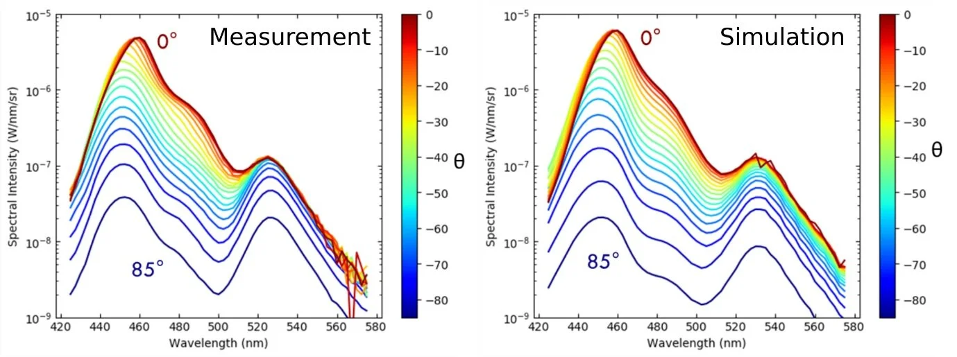
Figure 4: Measured (left) and simulated (right) angular emission spectrum of the OLED+QD stack. Setfos with the included ray-tracer is able to simulate even small details of the emission characteristics.
The simulation can now be used to optimize not only the perovskite quantum dot scattering layer but also the background light source. Figure 5 shows an example of switching the light source, the prediction using Setfos, and a measurement. This demonstrates that Setfos and its ray-tracing engine can be used to predictively simulate perovskite down conversion layers together with an arbitrary backlight unit.

Figure 5: Switching the light source to a laser diode (left), the simulation result to predict the angular emission spectrum (middle) and the measurement using the perovskite quantum dot film. This shows that the ray tracing engine in Setfos can be used to predict and optimize light down-conversion in quantum dots.
If we have sparked your interest to measure, simulate and optimize perovskite quantum dot films using Phelos and Setfos, get in contact with us or directly order a free of charge trial version of Setfos
References:
Semonin, O. E., Luther, J. M. & Beard, M. C. Quantum dots for next-generation photovoltaics. Mater. Today 15, 508–515 (2012).
Hao, M. et al. Ligand-assisted cation-exchange engineering for high-efficiency colloidal Cs1−xFAxPbI3 quantum dot solar cells with reduced phase segregation. Nat. Energy 5, 79–88 (2020).
Blülle, B. et al. 37.4: Light conversion and scattering properties of QD films for display applications: Angle‐resolved optical spectroscopy and numerical simulation. SID Symp. Dig. Tech. Pap. 50, 407–410 (2019).