Perovskite solar cell upscaling prediction
Emerging thin-film photovoltaic solar cells (like perovskites and organic) are the ideal candidate for large-area flexible applications. However, as discussed in a previous blog post, the total device resistance increases with the increase of the sample area, with a significant negative impact on the fill factor (FF). This effect can be compensated by lowering the sheet resistance (Rsheet) of the TCO with the addition of conductive metal grids on top of the TCO. This is increasing, in any case, the costs of production of the solar cell.
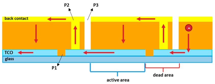
Figure1: monolithic module solar cell design.
An alternative solution to produce large-area photovoltaics is the so-called monolithic module design. It consists in dividing the active area of the sample into smaller cells with an interconnection gap. The photoactive layer is split into several electrically isolated subcells connected to one another through the top and bottom electrodes (see Figure 1 [Cas22]).
The narrower the subcell, the lower the resistance of each subcell with consequent improvement of the FF, but the interconnecting gap between each subcell is a “dead area”, which reduces the total active area of the module. The interconnection is fabricated by scribing the lines P1, P2, and P3, which respectively separate the TCO, the photoactive layer, and the top contact between consecutive subcells.
Clearly, there is a thread between the area of the single solar cell and the number of interconnections included in the device. Generally, the optimization of the module is done by experimental trial-and-error design.
Here, we are showing how to use the simulation software Laoss to predict which subcell area maximizes the power output of a mini-module with a total area of 50x41 mm2. This procedure is scalable to any module size and offers a valid alternative to the time-consuming experimental trial-and-error approach.
The 2D + 1D software LAOSS combines a 1D layer stack with 2D lateral simulations. The basic assumption is that the lateral flow of the current only occurs in the electrodes of the solar cell (2D simulation). Experimentally determined JV curves of lab-scale PSC devices provide the 1D coupling law that connects the two electrodes. The scale-up prediction of the JV characteristics for the mini-module is based on the experimental JV curve of the lab-scale device.
Do you want to learn more about Laoss?
Upscaling of ideal lab-scale solar cells
The scale-up prediction presented in this blog post is based on the experimental JV curves provided by the University of Surrey of lab-scale slot-die-coated perovskite solar cells with an active area of 0.25 cm2. The TCO of the module is an ITO layer with an Rsheet of 15 Ω/□ and the silver top contact has an Rsheet of 0.159 Ω/□.
Figure 2 (left) represents the module layout imported in Laoss. This is the top view of the module shown in Figure 1 with top and bottom contacts at the extreme right and left of the geometry, respectively, and an interconnection gap width of 2mm. Figure 2 (right) is a screen capture of the Laoss user interface with Rsheet values for the top and bottom interface of each subdomain. In the imported geometry, we defined the width of five subdomains: the top and bottom contact of the modules, the active area of the photoactive material, and the three scribing lines P1, P2, and P3.

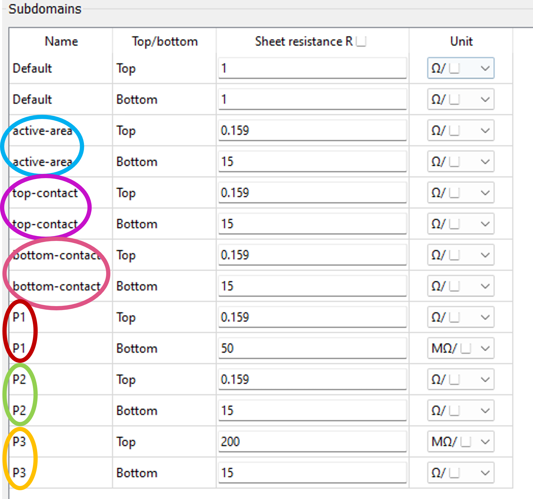
Figure 2: screenshots of Laoss software. (left) top-view of monolithic module with color bands highlighting P1, P2, P3 scribing lines, active area, top and bottom contact. (right) sheet resistances of the respective P1, P2, P3 scribing lines, active area, top and bottom contact.
Optimizing the design of a solar cell module requires the design of several module layouts with varying subcells and interconnection gap widths. This procedure is more precise but requires a considerable amount of work. With the feature “Full Module Handling” of Laoss, it is possible to perform simulations of modules of various sizes. The area of the subcells is defined by the height and width of the full module, the interconnection gap size, and the number of cells. However, the calculation of the IV curve for the full module assumes that the subcells are connected in series with no interconnection losses, hence a possible overestimation of the key figures, e.g. current and voltage, compared to the module design in Figure 2.
Figure 3 compares simulated JV curves for a module with 5-sub cells and an interconnection gap of 2mm as obtained with the Full module handling feature (blue curve) and for the effective module layout shown in Figure 2 (orange line). The 1D coupling law of both simulations is based on the same experimental lab-scale JV curve. Despite the assumption of a perfect interconnection with the Full module handling feature, the current density is only about 0.02 mA/cm2 higher at 0V, indicating that the full module handling provides a close approximation of the real module design.
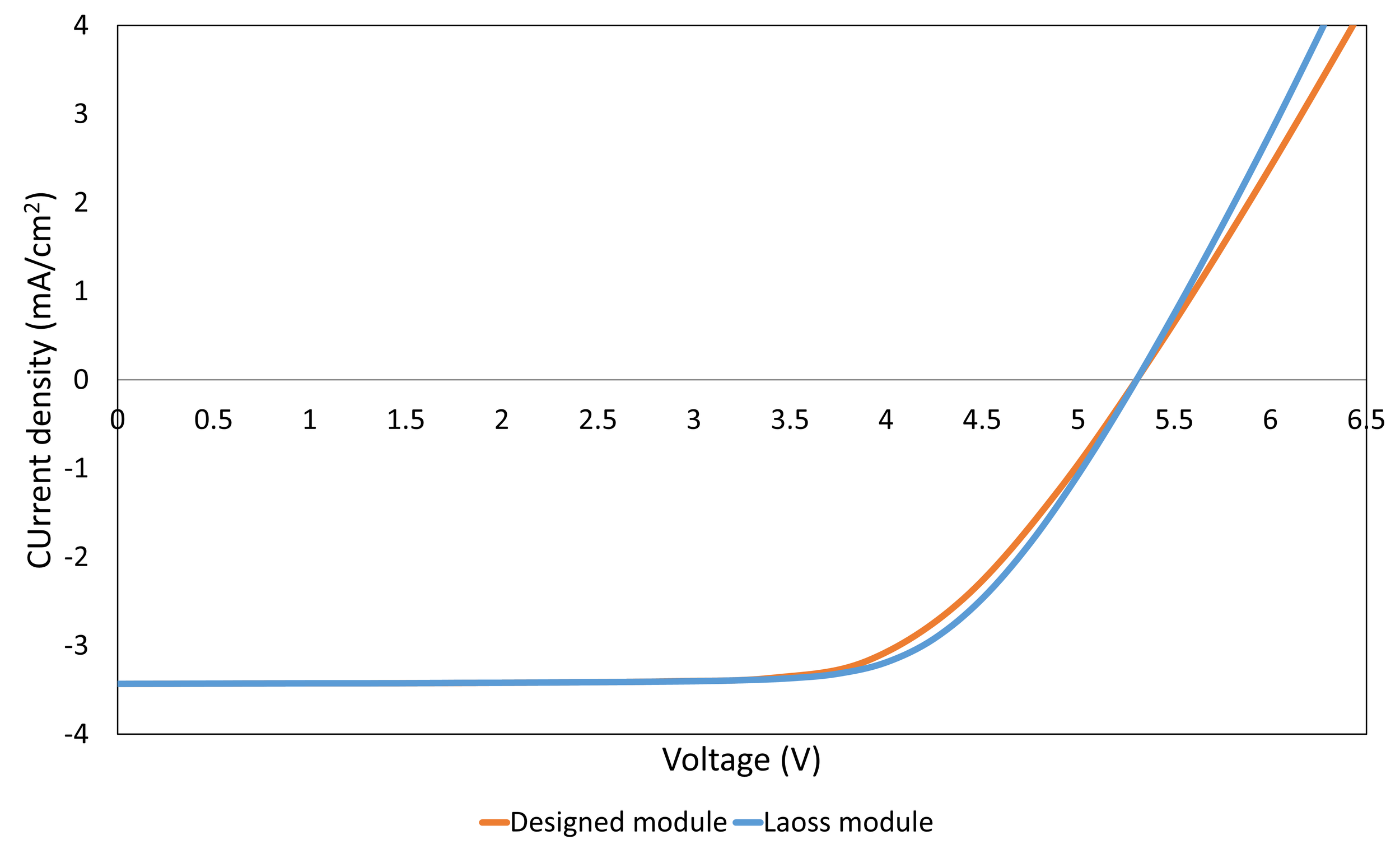
Figure 3: Simulated JV curves of a solar cell module with 5 sub cells based on the Full Module Handling approximation (blue line) and the effective module layout shown in Figure 2 (orange curve).

Figure 4: Full module handling feature in Laoss for predicting the ideal amount of sub cells in a monolithic module with defined geometry dimensions.
Figure 4 is a screenshot of the Full-module handling interface in Laoss. For the scale-up simulation, we considered a module height of 50mm and a module width of 41mm. The interconnection width (gap size) is fixed at 2mm, while the amount of subcells varies from one to 10.
Figure 5 shows the maximum power output that can be obtained with 4 subcells. With an increasing amount of subcells, the voltage increases linearly with more subcells according to Kirchhoff’s law of subcells connected in series (Figure 6). On the other hand, the current decreases due to the decreasing subcell area, hence a reduction in the total active area. The FF trend mirrors the current and is highest with 10 subcells because of the reduced total resistance.
In essence, the power output decreases with fewer than five subcells due to higher resistance and it decreases with more than five subcells due to the reduction in the active area (or increase in dead area).

Figure 5: Maximum power output per area with increasing number of sub cells for the monolithic module with 50x41mm2 substrate.


Figure 6: (left to right) Voc, Jsc and FF evolution with increasing number of sub cells for the monolithic module with 50x41mm2 substrate.
Influence of the Gap Width
As mentioned above, the interconnection gap is a non-active area (dead area). This must be reduced as much as possible to maximize the power output of the mini-module.
Figure 7 shows the maximum power output depending on the increasing number of subcells and with interconnection widths of 2mm (red curve), 1.5 mm (green curve), 1mm (blue curve), and 0.5mm (purple curve). Generally, with a narrower gap, the maximum power output is obtained for a larger amount of subcells.
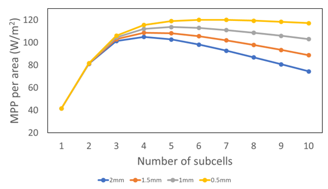
Figure 7: MPP vs number of sub cells for gap width of 2 mm (blue curve), 1.5 mm (orange curve), 1 mm (gray curve) and 0.5 mm (yellow curve).
It is interesting to observe that, for a given amount of subcells, by narrowing the gap also the FF decreases, due to a small increase in total resistance correlated with the increasing active area (Figure 8). On the other hand, the geometrical fill factor (GFF), the ratio of the active area with respect to the total module area, increases thanks to the reduction of dead area.

Figure 8: fill factor and geometrical fill factor for increasing gap width (2 mm (blue curve), 1.5 mm (orange curve), 1 mm (gray curve) and 0.5 mm (yellow curve)) and number of subcells.
A similar effect on the FF is obtained by decreasing the Rsheet of the TCO. Figure 9 shows the maximum power output with an increasing amount of subcells and Rsheet of 15 (blue line), 10 (orange line), and 5 (grey line) Ω/□. A lower Rsheet reduces the total series resistance of the cell as can be observed with the slope of the JV curve close to the Voc (Figure 9 top). A lower total resistance improves the squareness of the JV curve, hence the power at MPP increases and therefore the FF. Additionally, with a lower Rsheet the maximum power output is obtained for a smaller amount of subcells.
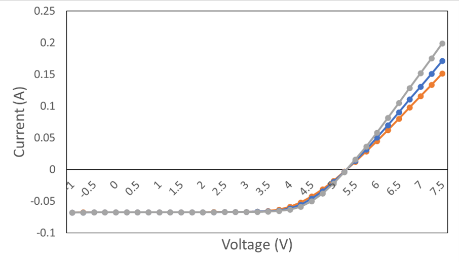

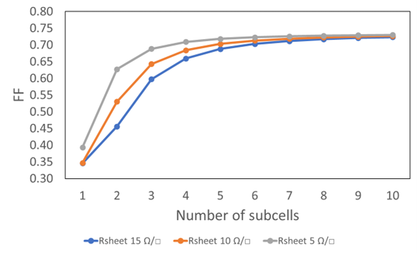
Figure 9: JV (top-left), MPP (top-right) and FF (bottom-left) for increaseing number of subcells and Rsheet of 15 Ω/□ (blue curve), 10 Ω/□ (orange curve) and 5 Ω/□ (gray curve).
Figure 10 shows the power density losses with various gap widths and Rsheet values compared to the lab-scale solar cell. For a module with a gap width of 2mm and Rsheet of 15 Ω/□, the loss in power density is more than 20% compared to the lab-scale cell. The steepness of the loss curve (orange line) represents the loss rate and we can observe that the reduction of dead area for a module with high sheet resistance (15 Ω/□) is more effective than reducing the sheet resistance with a smaller dead area (0.5mm gap).

Figure 10: MPP and power density losses with various gap widths and Rsheet values compared to the lab-scale solar cell.
Conclusions
In the first blog post on upscaling thin-film solar cells, we explained how the resistance of the TCO causes performance loss with increasing device area and how to minimize it with the addition of a metallic grid. In this second blog, we presented the concept of the monolithic module. This design introduces a dead area to separate the photoactive area into multiple subcells of smaller areas. The resistance is therefore reduced thanks to the smaller area, however also the current decreases.
The highest power output requires the optimization of the number of subcells and the width of the dead area to minimize the resistance and maximize the current. Despite the straightforward understanding of the observed effects, the use of module simulations is essential to find the optimum as this is not universal and depends on many parameters such as the PV stack (1D coupling law), the electrode resistance, the total module area, the interconnection width, and potentially others. The simulation software Laoss with its embedded Full Module Handling feature was instrumental in quickly optimizing the monolithic module design starting from the experimental JV curve of the lab-scale solar cell.
This study was carried out during the Musicode project.