Filter by: All | OLED | Solar Cell | Light Scattering | Drift Diffusion | Optics | Perovskite | Batteries | OLEC | Stability | Photodetectors
Simon J. Zeder, Balthasar Blülle, Beat Ruhstaller, and Urs Aeberhard, Opt. Express 32, 34154-34171 (2024)
https://doi.org/10.1364/OE.522953
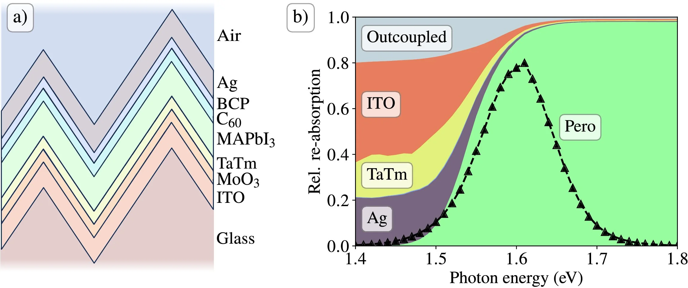
This paper presents a multiscale optical model developed to accurately quantify photon recycling (PR) and luminescent coupling (LC) in optoelectronic devices such as solar cells and LEDs. Photon recycling, the process of photon emission, re-absorption, and re-emission, can significantly enhance device efficiency, particularly in materials like GaAs, metal halide perovskites and even crystalline silicon. To accurately account for re-absorption effects, the model treats light absorption and emission equally, considering the full spectrum of internal modes within the device. This approach stands out from conventional methods, which focus solely on exterior-coupled modes.
The framework integrates two key propagation models:
Coherent Wave-Optical Model: Applied to thin-film layers where light interference effects are significant, avoiding unphysical divergencies for emitters embedded in absorbing media and ensuring consistency with detailed balance principles.
Incoherent Ray-Optical Model: Used for optically thick layers where coherence is lost, treating phase relations as irrelevant.
The model also accounts for light scattering at textured surfaces, essential for devices like perovskite –silicon tandem solar cells. By merging these approaches, the paper provides a robust framework for computing local emission, re-absorption, and energy flux rates in devices with complex structures. Importantly, this allows for a detailed understanding of the impact of photon recycling on device performance, including enhanced external quantum efficiency (EQE) in LEDs and increased open-circuit voltages in solar cells.
The model is validated through comparisons with analytical solutions, showing excellent agreement, and applied to a textured perovskite solar cell showcasing its capabilities. This validation confirms that the model can reliably be applied to real-world devices, offering a powerful tool for optimizing the performance of next-generation optoelectronic systems.
Key Takeaways:
∙ Comprehensive multiscale approach merging coherent and incoherent light models.
∙ Applicability to complex textured devices like perovskite solar cells and LEDs.
∙ Quantification of local re-absorption and energy flux rates.
∙ Validation through comparison with analytical solutions.

W.-H. Hu, F. Nüesch, D. Giavazzi, M. Jafarpour, R. Hany, M. Bauer, . Adv. Optical Mater. 2024, 12, 2302105. https://doi.org/10.1002/adom.202302105
This research focuses on using squaraine dyes in single-component shortwave infrared (SWIR) photodiodes and upconversion photodetectors. These devices achieve over 40% external quantum efficiency beyond 1000 nm through field-assisted exciton dissociation. By integrating SWIR photodiodes with organic LEDs, they convert SWIR photons into visible light, offering an alternative to inorganic imaging technologies.
Key Points
Efficient SWIR Detection: Over 40% external quantum efficiency beyond 1000 nm.
Field-Assisted Charge Generation: Enables efficient exciton dissociation.
Upconversion Photodetectors: Combine SWIR photodiodes with OLEDs for visible light emission.
Simplified Fabrication: Single-component layers enhance stability and reduce complexity.
Inorganic Alternative: Potential replacement for existing inorganic SWIR imaging technologies.
How Setfos Was Used
Setfos was employed for optical simulations, analyzing device layer properties using refractive index and extinction coefficient values. These simulations optimized light absorption and exciton generation, crucial for efficient SWIR detection and upconversion.

Morteza Najarian, A., Vafaie, M., Chen, B. et al.
Nat Rev Phys6, 219–230 (2024).
https://doi.org/10.1038/s42254-024-00699-z
This paper from the research team at the University of Toronto reviews materials suitable for high-speed photodetectors, emphasizing their photophysical characteristics. It covers material classes such as organic semiconductors, perovskites, and quantum dots, discussing their performance metrics, advantages, and limitations for applications in high-speed optical communication and imaging technologies.
How Setfos was used
Simulations to understand the dynamics of electron traps were conducted using SETFOS software.
Sami Toikkonen, G. Krishnamurthy Grandhi, Shaoyang Wang, Bora Baydin, Basheer Al-Anesi, L. Krishnan Jagadamma, Paola Vivo.
Adv Devices Instrum.2024;5:0048.
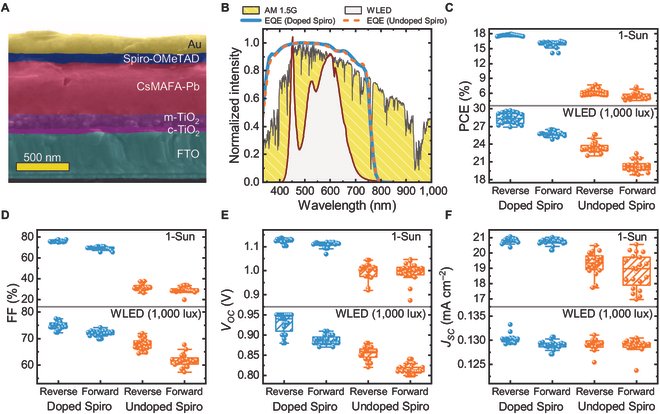
The study investigates the necessity of doping Spiro-OMeTAD in lead halide perovskite (LHP) indoor photovoltaics (IPVs). It concludes that undoped Spiro-OMeTAD can achieve high efficiency and stability under low-light conditions, rivaling doped counterparts, suggesting that dopants may not be essential for effective IPV performance.
How Litos Lite was used
Litos Lite was utilized to perform J–V reverse and forward sweeps (scan rate 50 mV s−1), maximum power point (MPP) tracking, and stable power output (SPO) measurements on the prepared photovoltaic cells. These measurements were conducted under both simulated sunlight (AM 1.5G, 1-Sun, 100 mW cm−2) and indoor WLED illumination (5,000 lux, ≈1.60 mW cm−2) in N2 atmosphere. The indoor MPP tracking was performed either under continuous illumination or in 8-hour light–16-hour dark cycles .
How Paios was used
Transient photovoltage and transient photocurrent measurement were carried out with the all-in-one characterization platform, Paios.

E. Benvenuti, A. Lanfranchi, S. Moschetto, M. Natali, M. Angelini, P. Lova, F. Prescimone, V. Ragona, D. Comoretto, M. Prosa, M. Bolognesi and S. Toffanin,
J. Mater. Chem. C, 2024,
This paper presents the development of an all-organic, on-chip integrated system for fluorescence detection, combining organic photodiodes (OPDs), organic light-emitting diodes (OLEDs), and a polymeric distributed Bragg reflector (DBR) filter. By integrating these components on a single substrate, the system offers a compact and efficient solution for fluorescence sensing, which is crucial for applications ranging from food safety to environmental monitoring. The use of organic materials allows for low-cost, flexible sensors that can be easily produced and deployed. The paper demonstrates that this integrated approach significantly enhances the optical efficiency and sensitivity of the fluorescence sensor, making it capable of detecting concentrations as low as 9.2 μM of the model dye Rhodamine 700. This advancement represents a significant step towards the development of portable, high-performance sensors for point-of-need applications
How Sefos was used
Setfos was used to design the OLED structure to achieve an efficient and narrow phosphorescent emission, crucial for the integrated fluorescence sensor's performance. The simulation helped in fine-tuning the composition and thickness of the OLED's interlayers, including an organic index matching layer, to enhance light extraction and emission characteristics tailored to the absorption spectrum of the fluorescent dye, Rhodamine 700.

Darshan H. Parmar, Benjamin Rehl, Ozan Atan, Sjoerd Hoogland, and Edward H. Sargent
ACS Applied Materials & Interfaces Article ASAP
DOI: 10.1021/acsami.3c14611
Colloidal quantum dot photodetectors exceed silicon's limits by detecting longer wavelengths, with performance depending on the ligand concentration during processing. This study connects simulated and actual photocurrent responses, showing that different ligand concentrations uniquely impact trap state density and device behavior.
How Setfos was used
Setfos was used to show how the transient measurements were consistent with a changing trap density in the photodetector active layer with respect to ligand exchange concentration.

Yu Zhang, Weiqing Nie, Mengli Hu, Wu Liu, Heng Liu, Xiaomin Huo, Yao Lu, Dandan Song, Bo Qiao, Zhiqin Liang, Zhiqiang Jiao, Zheng Xu, Guangcai Yuan, and Suling Zhao
ACS Photonics 2023 10 (10), 3521-3530
https://doi.org/10.1021/acsphotonics.3c00524
This research outlines the advancement in tandem optoelectronic devices, specifically a perovskite/organic quasi-tandem system for narrowband photodetectors (NPDs) targeting the visible to near-infrared spectrum. By varying the composition of perovskite and organic layers, the spectral response is tunable, enhancing device selectivity and flexibility. Achieving a peak response near 790 nm with a 41 nm bandwidth, these NPDs exhibit rapid submicrosecond response times, significantly outperforming traditional thick-layer photodetectors, marking a step forward in the development of ultra-fast NPDs.
How Setfos was used
Setfos was utilized to stimulate the penetration of different monochromatic light, the thickness of perovskite (MAPbI3) was set as 1700 nm, and a 150 nm of organic blend layer (PM6:IT-4F) was set on the perovskite. Take thickness as the scanning parameter, with a step size of 10 nm. The optical parameters (n, k) of the materials are obtained through an ellipsometer.

Jinno, H., Shivarudraiah, S. B., Asbjörn, R., Vagli, G., Marcato, T., Eickemeyer, F. T., Pfeifer, L., Yokota, T., Someya, T., Shih, C.-J.,
. Adv. Mater. 2023, 2304604.
https://doi.org/10.1002/adma.202304604
This research presents a breakthrough in ultrathin, flexible skin optoelectronics for Internet of Things (IoT) applications. Traditional issues like underperformance due to low polymer process temperatures and spectral distortion from bending are overcome using solution-processed perovskite semiconductors. The study introduces high-efficiency perovskite solar cells and LEDs on polymer films with exceptional thermal stability, achieving record efficiencies (18.2% for solar cells, 15.2 cd A−1 for LEDs) and bending-resistant light emission. This advancement enables reliable, high-performance, self-powered wearables and IoT sensors, demonstrating practical applications such as accurate pulse monitoring at a high selectivity rate.
How Setfos Was used
Finite element analysis for ultraflexible LED was simulated with the Setfos emission module. By expecting the dipole emission model of LED, the module allows to deliver emission spectra of ultraflexible LED with different angle.
Zhang, Z., Wang, L., Bi, H., Baranwal, A. K., Kapil, G., Sanehira, Y., Liu, J., Liu, D., Shen, Q., Hayase, S.,
Adv. Optical Mater. 2023, 2300962.
https://doi.org/10.1002/adom.202300962
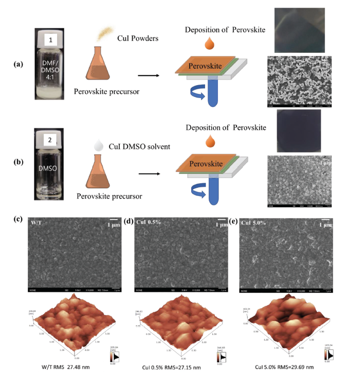
To enhance the efficiency of tin halide perovskite solar cells (PKSCs), researchers addressed defects like Sn4+ and iodide vacancies by introducing copper iodide (CuI) doping. A preprocessing method for CuI improved perovskite layer quality, resulting in efficiency increases from 9.8% to 13.1% for P-I-N structures and 9.4% to 10.5% for hole transport layer (HTL)-free structures. These doped tin-PKSCs also exhibited improved stability, retaining 75% of their initial power conversion efficiency after 102 days of storage.
How Paios was used
Intensity-modulated photovoltage spectroscopy (IMVS), Intensity-modulated photovoltage spectroscopy (IMPS), Transient photovoltaic voltage (TPV), and Transient photovoltaic current (TPC) were carried out via PAIOS software.

Abu Bakar Siddik, Epimitheas Georgitzikis, Yannick Hermans, Jubin Kang, Joo Hyoung Kim, Vladimir Pejovic, Itai Lieberman, Pawel E. Malinowski, Andriy Kadashchuk, Jan Genoe, Thierry Conard, David Cheyns, and Paul Heremans
ACS Applied Materials & Interfaces 2023 15 (25), 30534-30542
DOI: 10.1021/acsami.3c03708
This study presents a high-speed, low dark current near-infrared organic photodetector (NIR OPD) on a silicon substrate using amorphous indium gallium zinc oxide (a-IGZO) as the electron transport layer (ETL). Detailed characterization reveals the dark current mechanism as trap-assisted field-enhanced thermal emission, significantly reduced by introducing an interfacial layer. The NIR OPD achieves a low dark current of 125 pA/cm² at -1 V reverse bias and boasts a rapid photo response time, making it suitable for high-quality sample image capture in an imager on a complementary metal oxide semiconductor read-out circuit.
How Paios was used
Q-DLTS and TPV decay measurements were performed using Paios.

Zhou, X., Yan, Y., Zhang, F. et al.
J Mater Sci: Mater Electron 34, 1415 (2023).
https://doi.org/10.1007/s10854-023-10838-4
To enhance the performance and stability of organic solar cells (OSCs), a binary anode buffer layer strategy was employed using molybdenum oxide (MoO3) and PEDOT:PSS. This improved work function and interface contact, increasing the power conversion efficiency (PCE) from 16.25% to 17.34%. Additionally, MoO3 prevented direct contact between PEDOT:PSS and ITO, enhancing device stability. This approach offers a simple and efficient method for high-efficiency, stable OSCs suitable for commercial applications.

Lee, J., Georgitzikis, E., Hermans, Y. et al.
Nat Electron 6, 590–598 (2023).
https://doi.org/10.1038/s41928-023-01016-9
Thin-film image sensors with pinned photodiode structures, using organic or colloidal quantum dot photodiodes, demonstrate noise performance comparable to silicon-based counterparts. These sensors exhibit low noise, reduced dark current, high capacity, and efficient electron-to-voltage conversion. For instance, an organic absorber-based sensor achieves 54% quantum efficiency at 940 nm with 6.1e– read noise.
How Paios was used
The transient photoresponse, photocurrent linearity and capacitance–voltage measurements were performed using a Paios all-in-one system by Fluxim.
Pengyu Su, Huan Bi, Du Ran, Li Liu, Wenjing Hou, Guangzhao Wang, Wenbing Shi,
Chemical Engineering Journal, Volume 472, 2023, 145077, ISSN 1385-8947,
https://doi.org/10.1016/j.cej.2023.145077
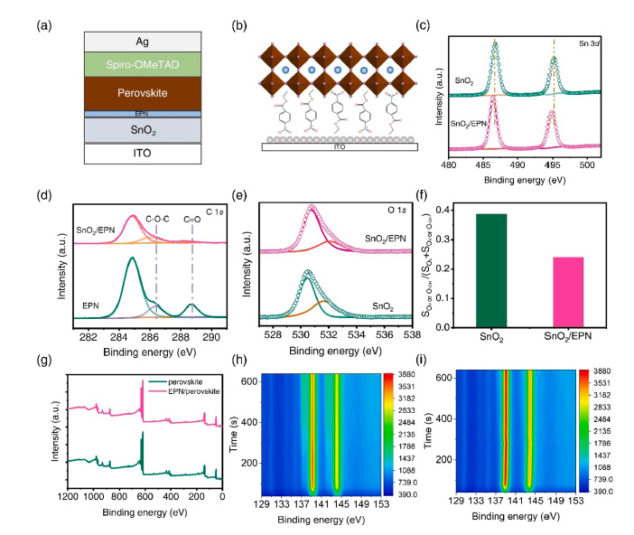
In a bid to enhance perovskite solar cell (PSC) performance and stability, a novel interfacial buffer layer called Ethyl p-nitrobenzoate (EPN) was introduced. EPN improved film quality, reduced defect density, relieved interfacial stress, and suppressed nonradiative recombination at the interface. This innovation led to a high 23.16% power conversion efficiency and improved device stability, showcasing the potential of multifunctional interfacial buffer layers in high-performance PSCs.
How Paios was used
TPC, TPV, IMPS, IMVS, and built-in potential were carried out via PAIOS in the structure of ITO/SnO2/(EPN)/perovskite/Spiro-OMeTAD/Ag, and the results were fitted using the companion software of PAIOS.

Montecucco, R., Pica, G., Romano, V., De Boni, F., Cavalli, S., Bruni, G., Quadrivi, E., De Bastiani, M., Prato, M., Po, R. and Grancini, G. (2023),
Sol. RRL 2300358.
https://doi.org/10.1002/adfm.202306040
All-inorganic perovskites show potential for creating stable and high-performing perovskite solar cells (PSCs). But, the high annealing temperature required for CsPbI3 stabilization limits its scalability for industrial production. This research introduces a method to stabilize CsPbI3ₓBrx perovskite at a reduced annealing temperature of 180°. This is achieved by using dimethylammonium (DMA) additives and bromide, facilitating the conversion to CsPbI3ₓBrx. Solar cells produced this way reached a power conversion efficiency (PCE) of 14.86%, outperforming the reference device. Using different halides in DMA salt for higher temperature annealing also proved beneficial, yielding an impressive PCE of 16.23%. This method, by lowering processing temperature, extends the utility of all-inorganic PSCs for industrial use and temperature-sensitive materials.
How Litos Lite was used
The stability measurements were performed at the MPP under N2 inert atmosphere and ambient temperature using Litos Lite coupled with a solar simulator continuously illuminating the devices. The spectrum used for the stability measurements was the same as the current density–voltage measurements.
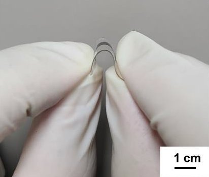
Kamijo, T., van Breemen, A.J.J.M., Ma, X. et al. A touchless user interface based on a near-infrared-sensitive transparent optical imager. Nat Electron (2023).
https://doi.org/10.1038/s41928-023-00970-8
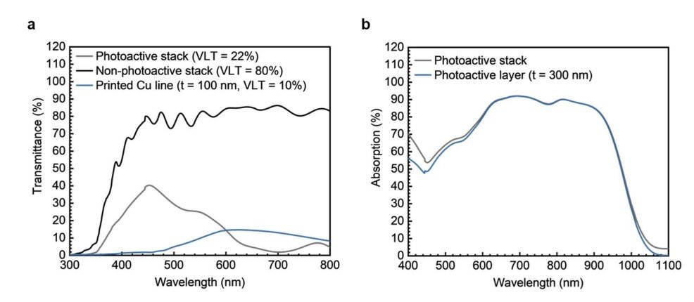
Researchers have developed a touchless user interface based on a visually transparent near-infrared-sensitive organic photodetector (OPD) array. The touchless interface can be used on top of a display, eliminating the need for physical contact.
The OPD array is designed with optical transparency in mind, using printed copper grids and patterned organic photodetector subpixels. The design optimization results in a high photodetectivity of 10^12 Jones at 850 nm and a visible-light transmittance of 70%.
The touchless user interface can be used with a penlight or through gesture recognition, providing a hygienic and convenient alternative to traditional touch screens. The technology has potential applications in automated teller machines (ATMs), ticket vending machines, and kiosks, where hygiene is a concern. It is a scalable and flexible solution that can be integrated into a variety of display applications without size limitations or calibration requirements. 2D FEM simulations for the surface potential and the current density distributions derived from the printed Cu grid structure .
How Fluxim’s Research Tools were used
Setfos
Numerical electro-optical simulations for the photogenerated J–V curves of our NIR-sensitive OPDs were performed by using Setfos.
The VLT of the parallel OPD subpixel array was calculated by the summation of the simulated optical transmittance for each component using Setfos
Laoss
2D FEM simulations for the surface potential and the current density distributions derived from the printed Cu grid structure for our NIR-sensitive OPDs were performed by Laoss 4.0
Shaoyang Wang et al 2023 J. Phys. Mater. 6 024004
Indoor photovoltaic devices using halide perovskites are studied for their potential in powering IoT applications. CH3NH3PbI3-based devices with Spiro-OMeTAD and P3HT as hole transport layers were compared, and Spiro-OMeTAD showed higher power conversion efficiency. The best-performing Spiro-OMeTAD device successfully powered a wearable motion sensor, demonstrating the potential for self-sufficient sensor systems.
Light intensity-dependent J-V measurement, transient photovoltage (TPV) and transient photocurrent (TPC) measurement were carried out with the characterization platform, Paios, Fluxim AG, Switzerland.

Metikoti Jagadeeswararao, Kyu Min Sim, Sangjun Lee, Mingyun Kang, Sanghyeok An, Geon-Hee Nam, Hye Ryun Sim, Elham Oleiki, Geunsik Lee, and Dae Sung Chung
Chemistry of Materials 2023 35 (8), 3095-3104
DOI: 10.1021/acs.chemmater.2c03271
This study demonstrates high-performance photomultiplication (PM)-type photodetectors using lead-free double perovskite, achieved by engineering trap states and trap-assisted charge injection. With a diode structure, the researchers realized selective hole traps, leading to high external quantum efficiency (EQE) of ∼16,000%, responsivity of ∼50 A W−1, and specific detectivity over 10¹² Jones at -3V. The work highlights PM photodetectors' potential through strategic trap engineering.
Setfos, a Fluxim software, was used for drift-diffusion simulations to gain comprehensive insight into the photomultiplication mechanism in the proposed photodetector.
Yi Yang, Jingwen Wang, Yunfei Zu, Qing Liao, Shaoqing Zhang, Zhong Zheng, Bowei Xu, Jianhui Hou,
Robust and hydrophobic interlayer material for efficient and highly stable organic solar cells,
Joule, Volume 7, Issue 3, 2023, Pages 545-557, ISSN 2542-4351,
https://doi.org/10.1016/j.joule.2023.02.013
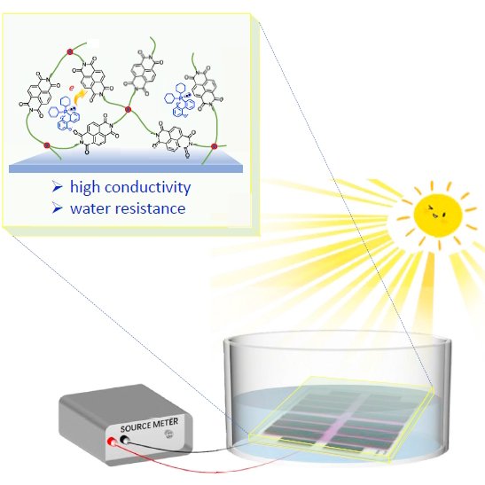
A robust, hydrophobic electron transporting interlayer for organic solar cells (OSCs) is designed using a cross-linkable naphthalene diimide (NDI) derivative. The non-polar electron donor PCy2 is used to n-dope the crosslinked c-NDI:PCy2 film, increasing its doping density and conductivity.
This hydrophobic interlayer protects the device against water, resulting in excellent water resistance. With the c-NDI:PCy2 interlayer, a power conversion efficiency of 17.7% is achieved, which is the highest for OSCs with an inverted device architecture. Notably, this OSC can be used underwater, maintaining 70% of its initial efficiency after 1,000 hours in the dark or 4 hours under continuous illumination.
Li, B., Huang, X., Wu, X., Zuo, Q., Cao, Y., Zhu, Q., Li, Y., Xu, Y., Zheng, G., Chen, D., Zhu, X.-H., Huang, F., Zhen, H., Hou, L., Qing, J., Cai, W., Adv. Funct. Mater. 2023, 2300216. https://doi.org/10.1002/adfm.202300216
Q-2D perovskites are promising photodetector materials, but their charge transport is limited by their hybrid low-dimensional structure. Researchers used a double-hole transport layer (PTAA & PEDOT:PSS) to create evenly-distributed 3D-like phases with vertical orientation, improving charge transport and reducing recombination.
This Ruddlesden-Popper perovskite photodetector achieved a high responsivity, specific detectivity, linear dynamic range, and fast rise/fall times. The study reveals the relationship between Q-2D perovskites' phase structure and performance, guiding future photodetector designs.
Transient photovoltage decay (TPV) measurements were performed with PAIOS instrumentation.
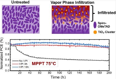
Andrés-Felipe Castro-Méndez, Jamie P. Wooding, Selma Fairach, Carlo A. R. Perini, Emily K. McGuinness, Jacob N. Vagott, Ruipeng Li, Sanggyun Kim, Vivek Brahmatewari, Nicholas Dentice, Mark D. Losego, and Juan-Pablo Correa-Baena
ACS Energy Lett. 2023, 8, 1, 844–852
Publication Date: January 3, 2023
https://doi.org/10.1021/acsenergylett.2c02272
This study investigates the use of vapor phase infiltration (VPI) to improve the stability of organic charge transport layers, such as hole-selective spiro-OMeTAD in perovskite solar cells (PSCs) and other organic electronic devices.
By using X-ray photoelectron spectroscopy (XPS), ultraviolet photoelectron spectroscopy (UPS), and grazing incident wide-angle X-ray scattering (GIWAXS), the study identifies that infiltration of TiOx via VPI hinders the crystallization of the spiro-OMeTAD layer. The infiltrated PSCs retained over 80% of their original efficiency after an operando stability test of 200 hours at 75°C, double the efficiency retained by devices without infiltration. This study suggests VPI can be used to stabilize organic charge transport layers and prolong device lifetimes.
Device stability measurements were carried out by tracking the maximum power point (MPP) of the devices while keeping constant the temperature of the films (by Peltier pads) at 75 °C using the stability measurement platform Litos from Fluxim.
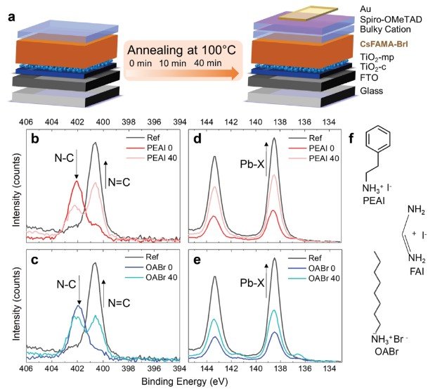
Carlo Andrea Riccardo Perini, Esteban Rojas-Gatjens, Magdalena Ravello, Andrés-Felipe Castro-Mendez, Juanita Hidalgo, Yu An, Sanggyun Kim, Barry Lai, Ruipeng Li, Carlos Silva-Acuña, and Juan-Pablo Correa-Baena
Adv. Mater. 2022, 34, 2204726
https://doi.org/10.1002/adma.202204726
This study investigates the impact of bulky-cation-modified interfaces on the stability of halide perovskite solar cells, which has not been extensively explored. The research demonstrates the thermal instability of these interface layers used in state-of-the-art solar cells and reveals changes in the chemical composition and structure of the films under thermal stress, which affects charge-carrier dynamics and device operation. The type of cation used for surface treatment also affects the extent of these changes, with long carbon chains providing more stable interfaces. The study emphasizes the importance of prolonged annealing of the treated interfaces to enable reliable reporting of performance and inform the selection of different bulky cations.
Device Characterization: The photovoltaic performance was evaluated using a Fluxim Litos Lite setup, equipped with a Wavelabs Sinus-70 AAA solar simulator with AM1.5 spectrum for excitation.
Aging tests were performed using a Fluxim Litos setup, using 1 Sun equivalent illumination with no UV-component, holding the substrates at 55 °C in a N2 atmosphere and using an MPP tracking algorithm. Every 12 h, a J–V scan in reverse and forward direction was automatically acquired.
Steele, J.A., Braeckevelt, T., Prakasam, V. et al.
Nat Commun 13, 7513 (2022).
https://doi.org/10.1038/s41467-022-35255-9
The black perovskite phase of CsPbI3 is promising for optoelectronic applications; however, it is unstable under ambient conditions, transforming within minutes into an optically inactive yellow phase, a fact that has so far prevented its widespread adoption.
In this paper the research team present an effective strategy for embedding an interfacial microstructure (a PbI2 microgrid) into stable CsPbI3 perovskite thin films and devices, using a coarse photolithographic approach. The microgrid is shown to dramatically increase the long-term stability of black CsPbI3 thin films (beyond 2.5 years in a dry environment) by increasing the phase transition energy barrier (Eb) and limiting the spread of potential yellow phase formation to a single, isolated domain of the grid.
Using stabilized photodetectors, integration of a microgrid into normally unstable planar CsPbI3 perovskite devices is shown to be a simple and effective strategy toward stable ambient operation.
Paios was used to measure the rise and decay time and the capacitance of the devices. The pulsed J-V characteristics were measured from 2 V to −1 V with 50 ms, 1 ms, and 25 ms as the pulse length, rise time, and measurement time, respectively.
Fan, B., Gao, W., Wu, X. et al.
Nature Communications 13, 5946 (2022).
doi.org/10.1038/s41467-022-33754-3
Power conversion efficiency and long-term stability are two critical metrics for evaluating the commercial potential of organic photovoltaics.
Although the field has witnessed a rapid progress of efficiency towards 19%, the intrinsic trade-off between efficiency and stability is still a challenging issue for bulk-heterojunction cells due to the very delicate crystallization dynamics of organic species. Herein, the research team from the City University of Hon Kong developed a class of non-fullerene acceptors with varied side groups as an alternative to aliphatic chains.
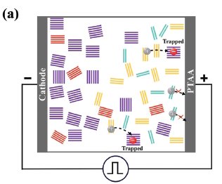
Delay-time charge extraction by linearly increasing voltage (CELIV) was measured on the all-in-one platform of Paios (FluximAG). A light pulse with duration of 50 μs generated from an 810 nm LED lamp (light intensity 100%) was applied prior to a voltage ramp of 1 V μs–1.
The delay time between light pulse and voltage ramp was varied from 0.2 to 10 μs. During the delay time, the open circuit was kept by applying the transient photovoltage signal to ensure no current is flowing.
Kunsik An, Chaewon Kim, Kwan Hyun Cho, Seunghwan Bae, Bo Kyung Cha, Kyung-Tae Kang,
Organic Electronics, Volume 100, 2022, 106384
doi.org/10.1016/j.orgel.2021.106384
An X-ray detector system was fabricated with an organic small molecule photodetector and a terbium-doped gadolinium oxysulfide (Gd2O2S:Tb) scintillating screen. Though the microsphere cluster structure of the Gd2O2S film had advantage in low material cost, wavelength matching to the proper photodetector is challenging due to its scintillating performance property in the relatively narrow emission spectrum range.
This work, including the spectral tuning using the strong microcavity effect and X-ray detection for medical applications, will provide new insights for the further development of OPDs.
The optical calculation of the absorption spectra was carried out using SETFOS. The optical constants n (refractive index) and k (absorption index) were obtained from the software.

Palepu Ashok, Jay Chandra Dhar
2022 International Conference for Advancement in Technology (ICONAT), 2022, pp. 1-6,
doi: 10.1109/ICONAT53423.2022.9725852.
Here the researchers designed an HTL free photo detector with ZnO as an electron transport layer (ETL) fabricated using RF sputtering and the perovskite material CH3NH3PbI3 as a light absorbing material deposited using two-step spin coating method.
The performance of the device is modelled by using SETFOS software with the impedance spectroscopy technique by changing different metal electrodes like, Ag, Au, Pd and Pt. Among all, the Pt electrode showed high current density (18.6914 mA/cm^2), high fill factor (0.558) and maximum power conversion efficiency (18.5%).

Qiwei Xu, I. Teng Cheong, Hanfa Song, Vien Van, Jonathan G. C. Veinot, and Xihua Wang
ACS Photonics 2022, 9, 8, 2792–2801
doi/pdf/10.1021/acsphotonics.2c00587
Integrating lead sulfide (PbS) colloidal quantum dots (CQDs) with crystalline silicon (c-Si) has been proven to be an effective strategy in extending the sensitivity of Si-based photodetectors into infrared regime. Here, the research team demonstrate the successful integration of PbS CQD inks with Si and construct a highly efficient heterojunction infrared photodiode operating in the range from 800 up to 1500 nm.
Summary points:
∙PbS CQD on Si to increase sensitivity of Si to IR
∙CQD:Si photodetector operating from 800 to 1500 nm
∙Layer of p-type QD enhances built-in electric field
∙EQE of 44% at 1280nm and 2V reverse bias - stable for more than 600 h
∙Photoresponse lower than 4μs without tails indicate low trap density
Lead sulfide (PbS) colloidal quantum dots (CQD) enable Si photodector sensitivity in the near infrared (NIR) in the range from 800 to 1500 nm.
The group of Xihua Wang at the University of Alberta achieved this result by spin-coating PbS CQD to form a CQD:Si heterojunction photodetector. The addition of a p-type CQD buffer layer at the CQD:Si interface enhanced the built-in electric field and improved the charge extraction. With transient photocurrent (TPC) and photovoltage (TPV) they measured a photoresponse lower than 4μs demonstrating low trap density at the CQD:Si interface.
TPC and TPV measurements were possible thanks to the all-in-one characterization platform PAIOS from Fluxim AG.
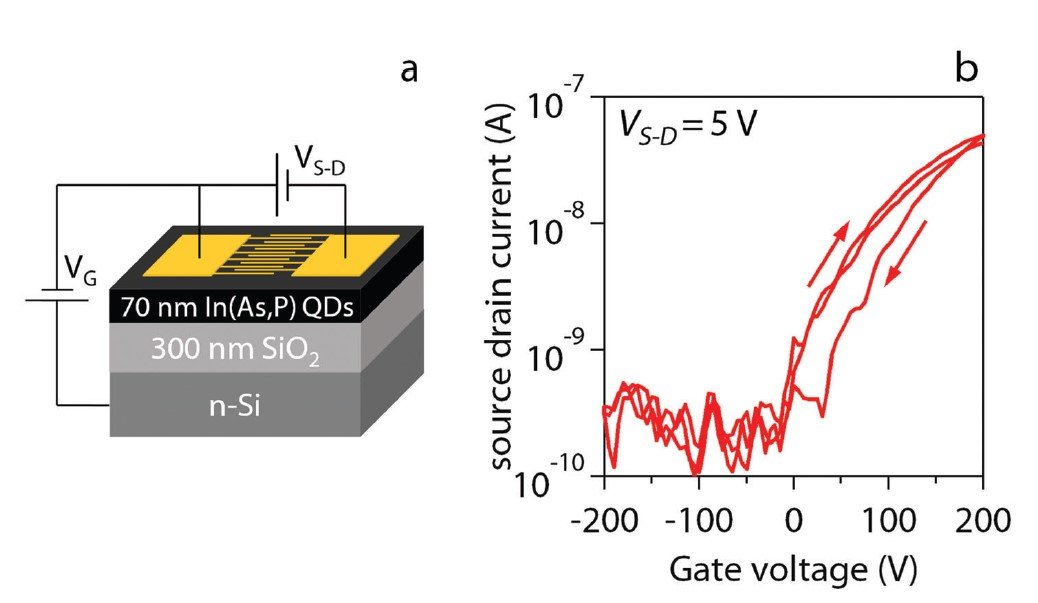
Leemans, J., Pejović, V., Georgitzikis, E., Minjauw, M., Siddik, A. B., Deng, Y.-H., Kuang, Y., Roelkens, G., Detavernier, C., Lieberman, I., Malinowski, P. E., Cheyns, D., Hens, Z.
Adv. Sci. 2022, 9, 2200844.
doi.org/10.1002/advs.202200844
QD-photodetectors are cost-effective, have small pixel pitch, and high spectral tunability, but they generally rely on restricted elements such as Pb and Hg. The team at Ghent University and imec fabricated high-efficiency photodetectors with non-restricted In(As,P) QDs deposited by spin-coating. These devices exhibit the best internal quantum efficiencies at the QD band gap of 46±5% and are sensitive to SWIR light up to 1400 nm.
Paios was used to characterize the photodetectors both in DC and transient modes. Thanks to all co-authors for your trust in our products.

Wei-Hsu Hu, Camilla Vael, Matthias Diethelm, Karen Strassel, Surendra B. Anantharaman, Abdessalem Aribia, Marco Cremona, Sandra Jenatsch, Frank Nüesch, and Roland Hany
Adv. Optical Mater. 2022, 2200695
Organic upconversion devices (OUCs) consist of an organic infrared photodetector and an organic visible light-emitting diode (OLED), connected in series. OUCs convert photons from the infrared to the visible and are of use in applications such as process control or imaging.
Many applications require a fast OUC response speed, namely the ability to accurately detect in the visible a rapidly changing infrared signal.
Here, high image-contrast, narrowband OUCs are reported that convert near-infrared (NIR) light at 980 and 976 nm with a full-width at half maximum of 130 nm into visible light. Transient photocurrent measurements show that the response speed decreases when lowering the NIR light intensity. This is contrary to conventional organic photodetectors that show the opposite speed-versus-light trend.
It is further found that the response speed increases (when using a phosphorescent OLED) or decreases (for a fluorescent OLED) when increasing the driving voltage.
To understand these surprising results, an analysis by numerical simulation is conducted. Results show that the response speed behavior is primarily determined by the electron mobility in the OLED. It is proposed that the low electron drift velocity in the emitter layer sets a fundamental limit to the response speed of OUCs.
Optical and electrical simulations were performed with Setfos 5.2
Vladimir Pejović, Epimitheas Georgitzikis, Itai Lieberman, Paweł E. Malinowski, Paul Heremans, David Cheyns
Adv Funct. Mat., (2022)
https://doi.org/10.1002/adfm.202201424
Image sensors based on colloidal quantum dots (CQDs) are expected to deliver affordable infrared image sensors to wider application scope. Here, a dual-band photodetector based on PbS CQDs is presented. By engineering the surface of CQDs, two oppositely facing pn junctions are fabricated in series, which enable sensing in two spectral channels. The presented photodetectors exhibit low dark current below 500 nA cm−2 at 1 V bias, a fast response measured in microseconds, as well as high external quantum efficiency, reaching 70% in NIR and 30% in SWIR.

Mingyun Kang, Syed Zahid Hassan, Seong-Min Ko, Changwon Choi, Juhee Kim, Santosh K. R. Parumala, Yun-Hi Kim, Yun Hee Jang, Jinhwan Yoon, Dong-Woo Jee, Dae Sung Chung
Advanced Materials
doi.org/10.1002/adma.202200526
When the intensity of the incident light increases, the photocurrents of organic photodiodes (OPDs) exhibit relatively early saturation, due to which OPDs cannot easily detect objects against strong backlights, such as sunlight. In this study, this problem is addressed by introducing a light-intensity-dependent transition of the operation mode, such that the operation mode of the OPD autonomously changes to overcome early photocurrent saturation as the incident light intensity passes the threshold intensity. The photoactive layer is doped with a strategically designed and synthesized molecular switch, 1,2-bis-(2-methyl-5-(4-cyanobiphenyl)-3-thienyl)tetrafluorobenzene (DAB). The proposed OPD exhibits a typical OPD performance with an external quantum efficiency (EQE) of <100% and a photomultiplication behavior with an EQE of >100% under low-intensity and high-intensity light illuminations, respectively, thereby resulting in an extension of the photoresponse linearity to a light intensity of 434 mW cm?2. This unique and reversible transition of the operation mode can be explained by the unbalanced quantum yield of photocyclization/photocycloreversion of the molecular switch. The details of the operation mechanism are discussed in conjunction with various photophysical analyses. Furthermore, they establish a prototype image sensor with an array of molecular-switch-embedded OPD pixels to demonstrate their extremely high sensitivity against strong light illumination.
To further verify the effect of DAB_c on gain generation, the researchers conducted a numerical simulation using the Fluxim’s Setfos software to fit the experimentally obtained OPD data and determine the relevant fitting parameters.